

基于SiP技术的高性能综合处理器电路设计
电子技术应用
汤明宏,苏龙,段玉贺
中国电子科技集团公司第五十八研究所
摘要: 随着后摩尔时代的来临,集成电路发展面临巨大的物理极限挑战,3D集成、先进封装等技术的出现,有效解决了半导体电路的集成度。研制了一款国产通用高性能综合处理器微系统电路,该电路采用国产化CPU+FPGA架构和三维立体集成封装工艺实现,内部集成NOR Flash、DDR3、千兆以太网收发器以及部分无源器件。采用三维立体集成封装工艺在保证电路性能的同时满足了小型化及大功耗散热的要求。测试结果表明,该电路能够实现5 Gb/s的SerDes接口的高速通信,处理器时钟频率达1.5 GHz,PCIe通信速率达5 Gb/s,实现了系统高性能及小型化的需求。
中图分类号:TN453 文献标志码:A DOI: 10.16157/j.issn.0258-7998.257712
中文引用格式: 汤明宏,苏龙,段玉贺. 基于SiP技术的高性能综合处理器电路设计[J]. 电子技术应用,2026,52(11):77-81.
英文引用格式: Tang Minghong,Su Long,Duan Yuhe. Design a high performance integrated processor circuit based on SiP technology[J]. Application of Electronic Technique,2026,52(11):77-81.
中文引用格式: 汤明宏,苏龙,段玉贺. 基于SiP技术的高性能综合处理器电路设计[J]. 电子技术应用,2026,52(11):77-81.
英文引用格式: Tang Minghong,Su Long,Duan Yuhe. Design a high performance integrated processor circuit based on SiP technology[J]. Application of Electronic Technique,2026,52(11):77-81.
Design a high performance integrated processor circuit based on SiP technology
Tang Minghong,Su Long,Duan Yuhe
No.58 Research Institute, China Electronics Technology Group Corporation
Abstract: In response to the requirements of miniaturization of high-end processors in the fields of flight control and guidance navigation, a domestically produced high performance integrated processor microsystem circuit is developed. The circuit adopts domestically produced domestic substitution CPU+FPGA architecture and three dimensional integrated packaging technology. It integrates NOR Flash, DDR3, Gigabit Ethernet transceivers, the use of three dimensional integrated packaging technology ensures circuit performance while meeting the requirements of miniaturization and high power consumption heat dissipation. The test results show that the circuit can realize the high speed communication of the 5 Gb/s SerDes interface, the processor clock frequency is 1.5 GHz, and the PCIe communication rate is 5 Gb/s, meeting the requirements of high performance and miniaturization of the system.
Key words : domestic substitution;high performance;system in package(SiP);miniaturization
引言
伴随着新一代武器装备的不断升级和指标需求的不断攀升,系统综合处理器电路的功能和性能也要得到不断完善和提高,同时,体积和重量却要求不断减小,以满足新型的装备的需求。功能的完备和性能的提高,带来了大量数据的处理,需要高性能的处理器完成相关的任务。体积和重量的减少,要求产品上的器件密度越来越高,对电路散热要求极高。采用微系统集成技术在满足数据处理能力的同时,可以将运算、缓存、存储、接口等进行高密度集成[1-2],既降低了各功能单元之间的互联损耗,又降低了信号处理单元的重量和体积,同时满足电路的散热要求。
本文采用系统级封装(System in Package, SiP)[3]技术将CPU、FPGA、DDR3、Flash、PHY等芯片以及若干阻容集成在一起,CPU为主控芯片,引导操作系统启动,FPGA提供CPU的上电时序,通过GTX接口实现SRIO、SerDes、SGMII等高速接口通信。
1 SiP电路设计难点及解决措施
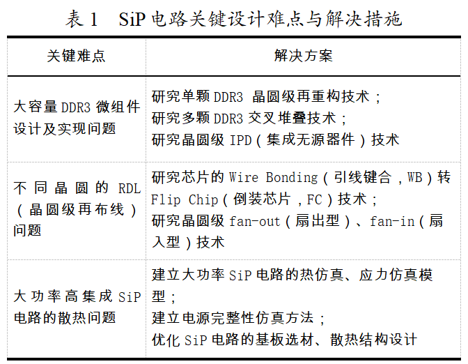
高性能综合处理器SiP电路对整个系统的散热及小型化、轻量化要求极高,传统的机载领域主控板卡重量和体积较大,无法满足新一代装备不断迭代升级的要求。与传统的控制系统不同,SiP电路的集成度更高,各个功能单元之间的互联损耗更低,涉及多种中道线工艺开发,这些问题也为大规模、高集成的SiP电路的研发带来诸多难点,表1列举了本文中SiP电路的关键难点和解决方案。
本文详细内容请下载:
https://www.chinaaet.com/resource/share/2000007349
作者信息:
汤明宏,苏龙,段玉贺
(中国电子科技集团公司第五十八研究所,江苏 无锡 214026)
此内容为AET网站原创,未经授权禁止转载。