ADI公司的ADu706x是全集成8kSPS取样速率24位数据采集系统,包括了高性能多路Sigma-Delta (Σ-Δ)模数转换器(ADC),16位/32位ARM7TDMI® MCU以及闪存/电可改写(EE)存储器.ADC具有2个差分对或4个单端通路,PGA(1-512)输入级,可选择输入范围从±2.34 mV 到 ±1.2 V,噪音30nV rms,主要用在工业自动化和过程控制,智能的精密的传感系统,基于4mA-20mA的智能传感器.本文介绍了ADuC706x主要特性,方框图和模拟方框图,以及采用精密模拟微控制器" title="模拟微控制器">模拟微控制器ADu7061/ADu7062的基于USB带冷结点补偿的热电耦" title="电耦">电耦温度监视器的应用电路和材料清单.
The ADuC706x series are fully integrated, 8 kSPS, 24-bit data acquisition systems incorporating high performance multichannel sigma-delta (Σ-Δ) analog-to-digital converters (ADCs), 16-bit/ 32-bit ARM7TDMI® MCU, and Flash/EE memory on a single chip.
The ADCs consist of a primary ADC with two differential pairs or four single-ended channels and an auxiliary ADC with up to seven channels. The ADCs operate in single-ended or differential input mode. A single-channel buffered voltage output DAC is available on chip. The DAC output range is programmable to one of four voltage ranges.
The devices operate from an on-chip oscillator and a PLL gene-rating an internal high frequency clock up to 10.24 MHz. The microcontroller core is an ARM7TDMI, 16-bit/32-bit RISC machine offering up to 10 MIPS peak performance; 4 kB of SRAM and 32 kB of nonvolatile Flash/EE memory are provided on chip. The ARM7TDMI core views all memory and registers as a single linear array.
The ADuC706x contains four timers. Timer1 is a wake-up timer with the ability to bring the part out of power saving mode. Timer2 is configurable as a watchdog timer. A 16-bit PWM with six output channels is also provided. The ADuC706x contains an advanced interrupt controller. The vectored interrupt controller (VIC) allows every interrupt to be assigned a priority level. It also supports nested interrupts to a maximum level of eight per IRQ and FIQ. When IRQ and FIQ interrupt sources are combined, a total of 16 nested interrupt levels is supported. On-chip factory firmware supports in-circuit serial download via the UART serial interface ports and nonintrusive emulation via the JTAG interface. The parts operate from 2.375 V to 2.625 V over an industrial temperature range of −40℃to +125℃.
ADuC706x主要特性:
Analog input/output
Dual (24-bit) ADCs
Single-ended and differential inputs
Programmable ADC output rate (4 Hz to 8 kHz)
Programmable digital filters
Built-in system calibration
Low power operation mode
Primary (24-bit) ADC channel
2 differential pairs or 4 single-ended channels
PGA (1 to 512) input stage
Selectable input range: ±2.34 mV to ±1.2 V
30 nV rms noise
Auxiliary (24-bit) ADC: 4 differential pairs or 7 single-ended channels
On-chip precision reference (±10 ppm/℃)
Programmable sensor excitation current sources
200 μA to 2 mA current source range
Single 14-bit voltage output DAC
Microcontroller
ARM7TDMI core, 16-/32-bit RISC architecture
JTAG port supports code download and debug
Multiple clocking options
Memory
32 kB (16 kB × 16) Flash/EE memory, including 2 kB kernel
4 kB (1 kB × 32) SRAM
Tools
In-circuit download, JTAG based debug
Low cost, QuickStart™ development system
Communications interfaces
SPI interface (5 Mbps)
4-byte receive and transmit FIFOs
UART serial I/O and I2C (master/slave)
On-chip peripherals
4× general-purpose (capture) timers including
Wake-up timer
Watchdog timer
Vectored interrupt controller for FIQ and IRQ
8 priority levels for each interrupt type
Interrupt on edge or level external pin inputs
16-bit, 6-channel PWM
General-purpose inputs/outputs
Up to 14 GPIO pins that are fully 3.3 V compliant
Power
AVDD/DVDD specified for 2.5 V (±5%)
Active mode: 2.74 mA (@ 640 kHz, ADC0 active)
10 mA (@ 10.24 MHz, both ADCs active)
Packages and temperature range
Fully specified for −40℃ to +125℃ operation
32-lead LFCSP (5 mm × 5 mm)
48-lead LFCSP and LQFP
Derivatives
32-lead LFCSP (ADuC7061)
48-lead LQFP and 48-lead LFCSP (ADuC7060)
ADuC706x应用:
Industrial automation and process control
Intelligent, precision sensing systems,
4 mA to 20 mA loop-based smart sensors
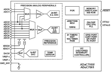
图1.ADuC706x功能方框图
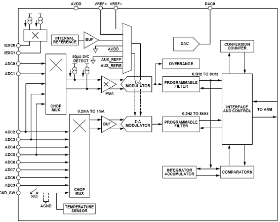
图2.ADuC706x模拟方框图
采用精密模拟微控制器的基于USB带冷结点补偿的热电耦温度监视器
This circuit uses the ADuC7060/ADuC7061 precision analog microcontroller in an accurate thermocouple temperature monitoring application. The ADuC7060/ADuC7061 integrates dual 24-bit Σ-Δ ADCs, dual programmable current sources, a 14-bit DAC, and a 1.2 V internal reference, as well as an ARM7 core, 32 kB flash, 4 kB SRAM, and various digital peripherals such as UART, timers, SPI, and I2C interfaces.
In the circuit, the ADuC7060/ADuC7061is connected to a thermocouple and a 100 Ω Pt RTD. The RTD is used for cold junction compensation.
In the source code, an ADC sampling rate of 100 Hz is chosen. When the ADC input PGA is configured for a gain of 32, the noise free code resolution of the ADuC7060/ADuC7061 is greater than 18 bits.
USB-Based Thermocouple Temperature Monitor with Cold Junction Compensation Using the ADuC7060/ADuC7061 Precision Analog Microcontroller (CN0214)
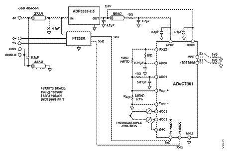
图3.ADuC706x温度监视控制器器热电耦接口
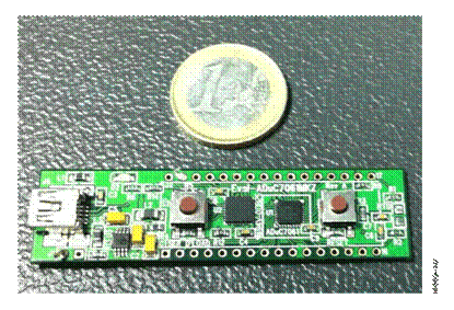
图4.EVAL-ADUC7061MKZ评估板" title="评估板">评估板外形图
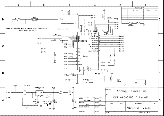
图5.EVAL-ADUC7061MKZ评估板电路图(1)
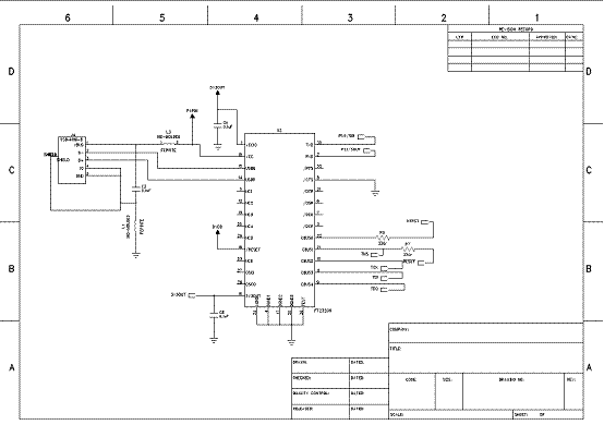
图6.EVAL-ADUC7061MKZ评估板电路图(2)

图7.EVAL-ADUC7061MKZ评估板测试建立框图
热电耦温度监视器材料清单见:
详情请见:
http://www.analog.com/static/imported-files/data_sheets/ADuC7060_7061.pdf
