
TIDS90C187平板电脑高清晰显示解决方案
TI 公司
摘要: TI公司的DS90C187是低功耗并串转换器(串化器),主要用在以电池为能源的手提设备,能降低主GPU和显示器间的RGB接口的尺寸.器件支持高达QXGA2048x1536@60Hz分辨率和主机和平板显示器间的双象素数据传输.185MHz时的功耗为100mW,能驱动QXGA/WQXGA显示器,支持24位RGB和48位RGB,有三种工作模式:单象素进/单象素出(SISO),单象素进/双象素出(SIDO)和双象素进/双象素出(DIDO).本文介绍了DS90C187主要特性,SISO,SIDO和DIDO功能框图,以及SIDO模
Abstract:
Key words :
</a>平板电脑" title="平板电脑">平板电脑" title="平板电脑">平板电脑和电子书系统方框图,C187EVK01评估模块(EVM)主要特性,电路图,材料清单和PCB布局图.
The DS90C187 is a Low Power Serializer for portable battery powered application that reduces the size of the RGB interface between the host GPU and the Display.
The DS90C187 Serializer is designed to support dual pixel data transmission between Host and Flat Panel Display up to QXGA 2048x1536@60Hz resolutions. The transmitter converts up to 48 bits (Dual Pixel 24 bit color) of 1.8V LVCMOS data into two channels of 4 data + clock (4D+C) reduced width interface LVDS compatible data streams.
DS90C187 supports 3 modes of operation. In single pixel mode in/out mode, the device can drive up to SXGA+ 1400x1050@60Hz. In this mode, the device converts one bank of 24 bit RGB data to one channel of 4D+C LVDS data stream. In single pixel in / dual pixel out mode, the device can drive up to WUXGA+ 1920x1440@60Hz. In this configuration,the device provides single-to-dual pixel conversion and converts one bank of 24 bit RGB data into two channels of 4D +C LVDS streams at half the pixel clock rate. In dual pixel in /dual pixel out mode, the device can drive up to QXGA 2048x1536@60Hz or up to QSXGA 2560x2048@30Hz. In this mode, the device converts 2 channels of 24 bit RGB data into 2 channels of 4D+C LVDS streams. For all the modes, the device supports 18bpp and 24bpp color.
The DS90C187 is offered in a small 92 pin dual row QFN package and features single 1.8V supply for minimal power dissipation.
DS90C187主要特性:
■ 100 mW typical power consumption at 185 MHz (SIDO mode)
■ Drives QXGA/WQXGA class displays
■ Three operating modes:
— Single Pixel In / Single Pixel Out (SISO), 105 MHz max
Single Pixel In / Dual Pixel Out (SIDO), 185 MHz
— Dual Pixel In / Dual Pixel Out (DIDO), 105 MHz
■ Supports 24 bit RGB, 48 bit RGB
■ Optional low power mode supports 18 bit RGB, 36 bit RGB
■ Supports 3D+C, 4D+C, 6D+C, 6D+2C, 8D+C, and 8D+2C LVDS configurations
■ Compatible with FPD-Link, and FlatLink Deserializers
■ 1.8V VDDIO & Core Supply
■ Interfaces directly with 1.8V LVCMOS
■ Less than 1mW power consumption in Sleep Mode
■ Spread Spectrum Clock Compatible
■ Small 7mm x 7mm x 0.9 mm 92–pin dual row QFN package
DS90C187应用:
■ Media Tablet Devices
■ eBook / Notebooks / Laptops
■ Portable Display Monitors

图1. DS90C187并串转换器方框图:单象素进/单象素出(SISO)

图2. DS90C187并串转换器方框图:单象素进/双象素出(SIDO)

图3. DS90C187并串转换器方框图:双象素进/双象素出(DIDO)
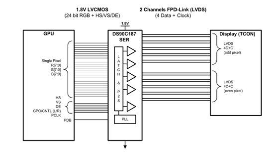
图4. DS90C187单象素进/双象素出(SIDO)模式应用电路
Tablet and eBook System Diagram
Texas Instruments (TI) offers a variety of semiconductor solutions for tablets and eBooks. The OMAP™ processor shown in the system diagram perfectly balances power and performance to give designers and end users an optimal multimedia solution. Also available are microprocessors from the Sitara™ ARM?Cortex?-A8 portfolio of microprocessors. In addition to processor technology, TI has invested in an extensive array of solutions for tablets and eBooks that support wireless connectivity, video, audio and power management. The selection guide on the following page is a sampling of TI devices available to streamline your design process.
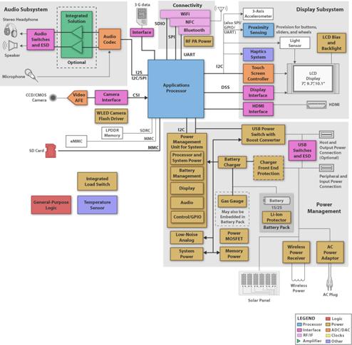
图5.平板电脑和电子书系统方框图
C187EVK01评估模块(EVM)
The Texas Instruments C187EVK01 evaluation module (EVM) helps designers evaluate the performance of the DS90C187 Low Power 1.8V Dual Pixel FPD-Link (LVDS) Serializer. The device operates off of a single 1.8V supply and supports input pixel clocks from 50 MHz to 185 MHz (Single In Dual Out) or 25 MHz to 105 MHz (Single/Dual In Single/Dual Out).
C187EVK01评估模块(EVM)主要特性:
100 mW typical power consumption at 185 MHz (SIDO mode)
Drives QXGA/WQXGA class displays
Three operating modes:
Single Pixel In/Single Pixel Out (SISO), 105 MHz max
Single Pixel In/Dual Pixel Out (SIDO), 185 MHz
Dual Pixel In / Dual Pixel Out (DIDO), 105 MHz
Supports 24 bit RGB, 48 bit RGB
Optional low power mode supports 18 bit RGB, 36 bit RGB
Supports 3D+C, 4D+C, 6D+C, 6D+2C, 8D+C, and 8D+2C LVDS configurations
Compatible with FPD-Link, and FlatLink Deserializers
1.8V VDDIO & Core Supply
Less than 1mW power consumption in Sleep Mode
Spread Spectrum Clock Compatible
Small 7mm x 7mm x 0.9 mm 92-pin dual row QFN package

图6. C187EVK01评估模块(EVM)外形图

图7. C187EVK01评估模块(EVM)电路图(1)

图8. C187EVK01评估模块(EVM)电路图(2)
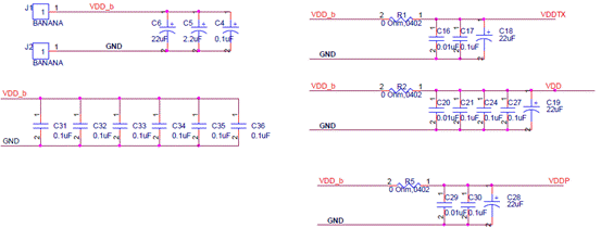
图9. C187EVK01评估模块(EVM)电路图(3)
C187EVK01评估模块(EVM)材料清单:
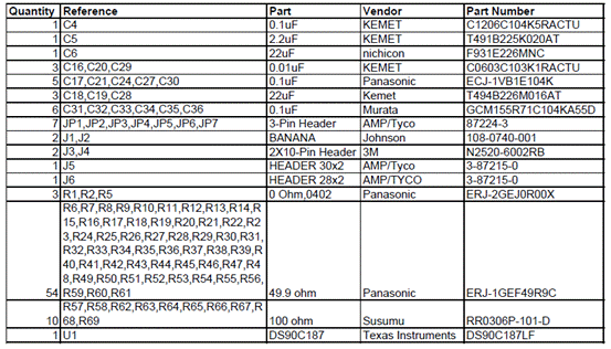

图10. C187EVK01评估模块(EVM)PCB布局图:顶层
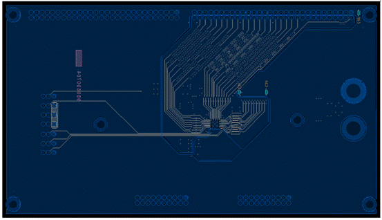
图11. C187EVK01评估模块(EVM)PCB布局图:底层
详情请见:
http://www.ti.com/lit/ds/symlink/ds90c187.pdf
和
http://www.ti.com/lit/ug/snlu102/snlu102.pdf
The DS90C187 is a Low Power Serializer for portable battery powered application that reduces the size of the RGB interface between the host GPU and the Display.
The DS90C187 Serializer is designed to support dual pixel data transmission between Host and Flat Panel Display up to QXGA 2048x1536@60Hz resolutions. The transmitter converts up to 48 bits (Dual Pixel 24 bit color) of 1.8V LVCMOS data into two channels of 4 data + clock (4D+C) reduced width interface LVDS compatible data streams.
DS90C187 supports 3 modes of operation. In single pixel mode in/out mode, the device can drive up to SXGA+ 1400x1050@60Hz. In this mode, the device converts one bank of 24 bit RGB data to one channel of 4D+C LVDS data stream. In single pixel in / dual pixel out mode, the device can drive up to WUXGA+ 1920x1440@60Hz. In this configuration,the device provides single-to-dual pixel conversion and converts one bank of 24 bit RGB data into two channels of 4D +C LVDS streams at half the pixel clock rate. In dual pixel in /dual pixel out mode, the device can drive up to QXGA 2048x1536@60Hz or up to QSXGA 2560x2048@30Hz. In this mode, the device converts 2 channels of 24 bit RGB data into 2 channels of 4D+C LVDS streams. For all the modes, the device supports 18bpp and 24bpp color.
The DS90C187 is offered in a small 92 pin dual row QFN package and features single 1.8V supply for minimal power dissipation.
DS90C187主要特性:
■ 100 mW typical power consumption at 185 MHz (SIDO mode)
■ Drives QXGA/WQXGA class displays
■ Three operating modes:
— Single Pixel In / Single Pixel Out (SISO), 105 MHz max
Single Pixel In / Dual Pixel Out (SIDO), 185 MHz
— Dual Pixel In / Dual Pixel Out (DIDO), 105 MHz
■ Supports 24 bit RGB, 48 bit RGB
■ Optional low power mode supports 18 bit RGB, 36 bit RGB
■ Supports 3D+C, 4D+C, 6D+C, 6D+2C, 8D+C, and 8D+2C LVDS configurations
■ Compatible with FPD-Link, and FlatLink Deserializers
■ 1.8V VDDIO & Core Supply
■ Interfaces directly with 1.8V LVCMOS
■ Less than 1mW power consumption in Sleep Mode
■ Spread Spectrum Clock Compatible
■ Small 7mm x 7mm x 0.9 mm 92–pin dual row QFN package
DS90C187应用:
■ Media Tablet Devices
■ eBook / Notebooks / Laptops
■ Portable Display Monitors
图1. DS90C187并串转换器方框图:单象素进/单象素出(SISO)
图2. DS90C187并串转换器方框图:单象素进/双象素出(SIDO)
图3. DS90C187并串转换器方框图:双象素进/双象素出(DIDO)
图4. DS90C187单象素进/双象素出(SIDO)模式应用电路
Tablet and eBook System Diagram
Texas Instruments (TI) offers a variety of semiconductor solutions for tablets and eBooks. The OMAP™ processor shown in the system diagram perfectly balances power and performance to give designers and end users an optimal multimedia solution. Also available are microprocessors from the Sitara™ ARM?Cortex?-A8 portfolio of microprocessors. In addition to processor technology, TI has invested in an extensive array of solutions for tablets and eBooks that support wireless connectivity, video, audio and power management. The selection guide on the following page is a sampling of TI devices available to streamline your design process.
图5.平板电脑和电子书系统方框图
C187EVK01评估模块(EVM)
The Texas Instruments C187EVK01 evaluation module (EVM) helps designers evaluate the performance of the DS90C187 Low Power 1.8V Dual Pixel FPD-Link (LVDS) Serializer. The device operates off of a single 1.8V supply and supports input pixel clocks from 50 MHz to 185 MHz (Single In Dual Out) or 25 MHz to 105 MHz (Single/Dual In Single/Dual Out).
C187EVK01评估模块(EVM)主要特性:
100 mW typical power consumption at 185 MHz (SIDO mode)
Drives QXGA/WQXGA class displays
Three operating modes:
Single Pixel In/Single Pixel Out (SISO), 105 MHz max
Single Pixel In/Dual Pixel Out (SIDO), 185 MHz
Dual Pixel In / Dual Pixel Out (DIDO), 105 MHz
Supports 24 bit RGB, 48 bit RGB
Optional low power mode supports 18 bit RGB, 36 bit RGB
Supports 3D+C, 4D+C, 6D+C, 6D+2C, 8D+C, and 8D+2C LVDS configurations
Compatible with FPD-Link, and FlatLink Deserializers
1.8V VDDIO & Core Supply
Less than 1mW power consumption in Sleep Mode
Spread Spectrum Clock Compatible
Small 7mm x 7mm x 0.9 mm 92-pin dual row QFN package
图6. C187EVK01评估模块(EVM)外形图
图7. C187EVK01评估模块(EVM)电路图(1)
图8. C187EVK01评估模块(EVM)电路图(2)
图9. C187EVK01评估模块(EVM)电路图(3)
C187EVK01评估模块(EVM)材料清单:
图10. C187EVK01评估模块(EVM)PCB布局图:顶层
图11. C187EVK01评估模块(EVM)PCB布局图:底层
详情请见:
http://www.ti.com/lit/ds/symlink/ds90c187.pdf
和
http://www.ti.com/lit/ug/snlu102/snlu102.pdf
此内容为AET网站原创,未经授权禁止转载。