
NS LM5015高压DC-DC稳压器方案
2008-01-29
作者:美国国家半导体
美国国半(NS )公司的LM5015是高压单片双开关" title="双开关">双开关的DC/DC开关稳压器,它包括了实现高压双开关正激" title="双开关正激">双开关正激和反激" title="反激">反激稳压器所需的所有功能,高边和低边集成了75伏N沟 MOSFET,峰值电流大于1 A。LM5015采用电流模式控制,开关频率可编程到750 kHz。输入电压从4.25V 到75V,广泛应用于通信,汽车电子以及工业控制。本文介绍了LM5015的主要性能,方框图,典型应用电路以及几种应用案例" title="应用案例">应用案例的详细电路图。
LM5015:High Voltage Monolithic Two-Switch Forward DC-DC" title="DC-DC">DC-DC Regulator
概述:
The LM5015 high voltage switch mode regulator features all the functions necessary to implement efficient high voltage Two-Switch Forward and Two-Switch Flyback regulators, using a minimum of external components. This easy to use regulator integrates high side and low side 75 Volt N-Channel MOSFETs with a minimum 1 Amp peak current limit. The voltage across the MOSFETs employed in the two-switch topology is clamped to the input voltage, allowing the input voltage range to approach the rating of the MOSFETs. The regulator control method is based on current mode control providing inherent ease of loop compensation and line feedforward for superior rejection of input transients.
The operating frequency is set with a single resistor and is programmable up to 750 kHz. The oscillator can also be synchronized to an external clock. Additional protection features include cycle-by-cycle current limiting, thermal shutdown, under- voltage lockout and remote shutdown capability. The device is available in the TSSOP-14EP package featuring an exposed die attach pad to enhance thermal dissipation.

主要特性:
■ Dual Integrated 75V N-Channel MOSFETs
■ Ultra-wide input voltage range: 4.25V to 75V
■ Integrated high voltage bias regulator
■ Adjustable output voltage
■ 1.5% feedback reference accuracy
■ Current mode control with selectable compensation
■ Wide bandwidth error amplifier
■ Integrated current sensing and limiting
■ 50% maximum duty cycle limit
■ Single resistor oscillator programming
■ Oscillator synchronization capability
■ Programmable soft-start
■ Enable / Under-voltage Lockout (UVLO) pin
■ Thermal shutdown
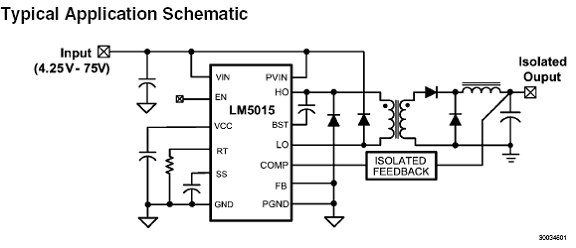
图1。LM5015典型应用电路图

图2。LM5015方框图
应用案例:
The following schematics present four examples dc-dc converters utilizing the LM5015 switching regulator IC:
1. Non-Isolated Two-Switch Forward for 48V input and 5V 2.5A output,
2. Isolated Two-Switch Forward for 48V input and 5V 2.5A output
3. Isolated Two-Switch Flyback converter for 48V input and 5V 2.5A output,
4. A 1:1 dc-dc transformer with the input/output operating range of 5V to 15V
一.48V NON-ISOLATED TWO-SWITCH FORWARD
The Non-Isolated Two-Switch Forward converter shown in Figure 3 utilizes the internal voltage reference for the regulation set-point. The output is +5V at 2.5A while the input
voltage can vary from 36V to 72V. The switching frequency is 300 kHz. An auxiliary winding on transformer (T1) provides 10V to power the LM5015 when the output is in regulation.
This disables the internal high voltage VCC LDO regulator and improves efficiency. The converter can be shut down by driving the EN input below 1.26V with an open-collector or open-drain transistor. An external synchronizing frequency can be applied to the SYNC input.

图3。48伏非绝缘双开关正激电路图
二.48V ISOLATED TWO-SWITCH FORWARD
The Isolated Two-Switch Forward converter shown in Figure 4 utilizes a 1.24V voltage reference (LMV431A) located on the isolated secondary side for the regulation set-point. The LM5015 internal error amplifier is disabled by grounding the FB pin. The LMV431A controls the current through the optocoupler LED, which sets the COMP pin voltage. The output is +5V at 2.5A and the input voltage ranges from 36V to 72V.
The switching frequency is 300 kHz. The functions of the EN and SYNC inputs are the same as in the previous example circuit.

图4。48伏绝缘双开关正激电路图
三.ISOLATED TWO-SWITCH FLYBACK
The Isolated Two-Switch Flyback converter shown in Figure 5 utilizes a 1.24V voltage reference (LMV431A) located on the isolated secondary side for the regulation set-point. The LM5015 internal error amplifier is disabled by grounding the FB pin. The LMV431A controls the current through the optocoupler LED, which sets the COMP pin voltage. The output is +5V at 2.5A and the input voltage ranges from 36V to 72V.
The switching frequency is 300 kHz. The Flyback converter is less complex than the previous Forward converter example in Figure 13. However, the Flyback converter produces higher input and output ripples of voltage and currents, and lower conversion efficiency by about 2%. The functions of the EN and SYNC inputs are the same as in the previous example circuits.
This circuit can be used with the LM5073 for a low cost isolated Power over Ethernet (PoE) Power Device (PD) application that does not require a discrete power MOSFET.
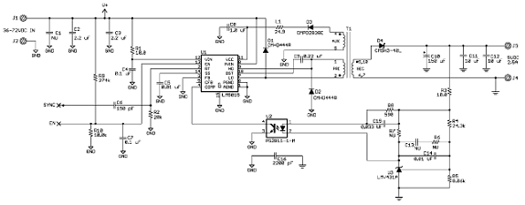
图5。绝缘双开关反激电路图
四.DC-DC TRANSFORMER
The DC-DC transformer shown in Figure 6 provides a 1:1 input voltage to output voltage conversion with ground isolation. The circuit operates in open loop manner operating at the maximum duty cycle limit of the LM5015. The power transformer primary-secondary turns ratio is 1:2 (primary to secondary). Therefore, at the maximum duty cycle of 0.5, the output voltage will be approximately equal to the input voltage.
A Zener diode Z1 is used at the output rail as a simple means to protect the output against over-voltage under light and no load conditions. The maximum load of this example circuit is 0.3A, and the operating voltage range is from 5V to 15V.
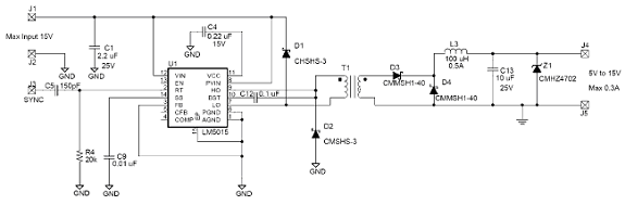
图6。变压器DC-DC转换器电路图