NXP 公司的PCF8811 是低功耗80x126象素CMOS LCD控制器,具有80行和128列输出,显示器数据RAM 80x128位,具有8位并行接口,3/4路SPI和高速I2C总线,适合于以电池为能源的系统,主要用于汽车显示器,通信设备,手提仪表和POS终端。本文介绍了PCF8811主要特性和优势,方框图,以及几种典型应用框图。
PCF8811:80 x 128 pixels matrix LCD driver
The PCF8811 is a low-power CMOS1 LCD controller and driver, designed to drive a graphic display of 80 rows and 128 columns or a graphic display of 79 rows and 128 columns and an icon row of 128 symbols. All necessary functions for the display are provided in a single chip, including on-chip generation of the LCD supply and bias voltages, resulting in a minimum of external components and low power consumption. The PCF8811 can interface microcontrollers via a parallel bus, serial bus or I2C-bus interface.
PCF8811主要特性和优势:
Single-chip LCD controller and driver
80 row and 128 column outputs
Display data RAM 80 × 128 bit
128 icons (row 80 can be used for icons in extended command set and when icon rows are enabled)
Low power consumption; suitable for battery operated systems
Interfaces: an 8-bit parallel interface, 3 or 4-line Serial Peripheral Interface (SPI) and High-speed I2C-bus
On-chip:
Configurable voltage multiplier generating LCD supply voltage VLCD; an external VLCD is also possible
Linear temperature compensation of VLCD; 8 programmable temperature coefficients (extended command set); one fixed temperature coefficient which can be set as default by OTP programming (basic command set)
Generation of intermediate LCD bias voltage
Oscillator requires no external components
OTP calibration for VLCD and accurate frame frequency
External reset input pad
External clock input possible
Multiplex rate: 1:16 to 1:80 in steps of 8 when no icon row is used; with the icon row, steps of 16 can be used
Logic supply voltage range VDD1 to VSS:
1.7 V to 3.3 V
High-voltage multiplier supply voltage range VDD2, VDD3 to VSS:
1.8 V to 3.3 V
Display supply voltage range VLCD to VSS:
3 V to 9 V
Programmable bottom row pads mirroring; for compatibility with both Tape Carrier Packages (TCP) and Chip-On-Glass (COG) applications (extended command set)
Status read, which allows for chip recognition and content checking of some registers
Start address line which allows, for instance, the scrolling of the displayed image
Programmable display RAM pointers for variable display sizes
Slim chip layout, suited for COG applications
Temperature range: Tamb = −40℃ to +85℃
CMOS compatible inputs
PCF8811应用:
Automotive displays
Telecom equipment
Portable instruments
Point-of-sale terminals
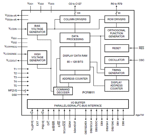
图1。PCF8811方框图
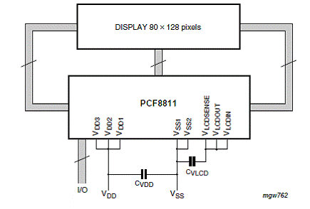
图2。PCF8811应用框图:内部电荷泵和单电源
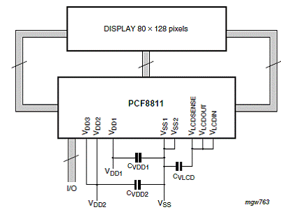
图3。PCF8811应用框图:内部电荷泵和两个分立电源(VDD1和VDD2)
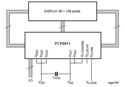
图4。PCF8811应用框图:外接高压
详情请见:
http://www.nxp.com/documents/data_sheet/PCF8811.pdf
