
仅需要少数廉价元器件,图1中的电路断路器响应过流和过压故障。电路的核心处,一个可调高精度的并联稳压器D2,提供参考电压、比较器和开集电极输出,所有功能都整合到三管脚的封装中。

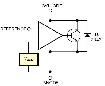
图2显示ZR431, D1的简化电路图。在参考输入处的电压与内部电压基准VREF相比较,名义上是2.5V。在断电状态下,参考电压为0V,输出晶体管处于截止状态,阴极电流小于0.1µA。随着参考电压接近VREF,阴极电流缓慢增加;参考电压超过2.5V的阈值时,装置完全导通,阴极电压降至大约为2V。在这种情况下,阴极和电源之间的阻抗决定阴极电流;阴极电流在50µA至100mA范围内。
在正常工作情况下,D2的输出晶体管截止,而且P沟道MOSFET(Q4)的门极通过R9,以至于MOSFET是全面增强的,允许负载电流ILOAD从电源–VS通过R6流到负载处。Q2和电流敏感电阻R6监测ILOAD的幅值,其中Q2的基极和发射极电压VBE是ILOAD×R6。对于ILOAD的正常值,VBE低于Q2偏置所需的0.6V电压值,
这种情况下晶体管对R3 和R4连结处的电压也没有影响。因为D2参考输入的输入电流小于1µA,通过R5可忽略压降,而参考电压实际上是R4上的电压。
当ILOAD超过最大允许值时发生过载情况,R6上的电压增大导致基极-发射极电压足够大到导通Q2。因此,R4上的电压和参考电压上拉到VS,造成D2的阴极电压降至大约2V。D2的输出晶体管通过R7 和 R8的泻放电流,因此偏置Q3导通。Q4的栅极电压通过Q3有效地控制电源,MOSFET从而截止。与此同时,Q3的源电流通过D1流到R4,从而拉动R4的电压,使二极管电压降到低于电源。由于Q2的基极-发射极的电压为0V而截止,因此没有负载电流流过R6。D2的输出晶体管锁存,电路仍处于故障状态,其中的负载电流为0A。选择R6的阻值时要确保在负载电流的最高允许值的条件下,Q2的基极-发射极电压大约低于0.5V。
对于过流情况,该断路器还对电源的非正常大电压起作用。当负载电流在正常范围内Q2处于截止状态时,电源幅值以及R3和R4的值,穿过电源轨形成潜在分压器,决定参考输入处的电压。电源电压发生过压情况,R4的电压超过2.5V参考电压,D2的输出晶体管导通。一旦再次发生,Q3导通,MOSFET(Q4)关闭,负载与危险瞬间情况有效隔绝。
现在电路仍然处在不定状态一直到复位。在这些条件下,Q3 控制 Q4的栅极电源电压大约接近0V,从而保护MOSFET自身摆脱过多的栅源电压。忽视R5微乎其微的电压值,你可以看到参考电压为VS×R4/(R3+R4)。因为,当参考电压超过2.5V时,D2的输出变高,你可以变换方程为R3=[(VST/2.5)–1]×R4,其中VST是所需的电源跳闸值。例如,如果R4值为10kΩ,18V的跳闸电压需要R3阻值为62kΩ。R3 和 R4选择适当的阻值来设置需要的跳闸电压值,确保它们足够大以至于潜在分压器不会过度负荷供应。同样,由于输入参考电流避免导致误差的值。
当你第一次对电路供电,会发现电容、灯泡灯丝、汽车等类似具有大浪涌电流的载荷可以使断路器跳闸,即使正常的、稳态运行的电流低于R6所设置的水平。解决这个问题的一个办法,就是增加电容C2,降低参考输入处电压的变化率。不过,虽然简单,但这种方式有一个严重的缺点,因为它减缓了电路对于真正过流故障的响应时间。
器件C1,、R1,、R2和Q1提供了另一种解决方法。当电压变大时,C1初始时放电,导致Q1导通,从而控制参考输入为0V,防止来自跳闸电路的涌电流。然后C1通过R1 和R2 充电,直到Q1最后截止,释放参考输入的控制,并允许电路快速反应过流瞬变。此时C1、R1和 R2的值,电路允许涌电流在大约400毫秒内平息下来。选择其它值可以使电路容纳适用于负载的任何时限的涌电流。一旦你的电路断路器跳闸,再次供电或者按下复位开关S1则可以复位。如果你的应用不需要涌电流保护,干脆省略C1、R1和 R2,并在参考输入和0V之间接入S1。
在选择元器件时,确保所有的元器件妥善适应它们将遇到的电压和电流水平。双极晶体管没有特别的要求,虽然这些晶体管,尤其Q2和Q3,应具有高电流增益,Q4应该有较低的阻值,并且Q4的最大漏源极电压和栅源极电压必须与最高电源电压相同。你可以为D1使用几乎任何一个小信号的二极管。作为一项预防措施,如果有非常大的瞬态电压,适当的齐纳二极管D3 和D4保护D2可能是有必要的。
虽然该电路利用431器件,是市面从不同厂家都有的广泛产品,对于D2,并不是所有这些产品都表现的一模一样。举例来说,测试了德州仪器的TL431CLP和Zetex公司的ZR431CLP,显示当参考电压为0V时两个器件的阴极电流是0A。但是,逐步把参考电压从2.2V提高到2.45V,对于TL431CLP而言,阴极电流由220提高到380µA,而ZR431CLP是从 23到28µA—两者大概有10种区别。在选择R7 和R8的阻值时,你必须考虑这两种不同大小的阴极电流的区别。
你所使用的D2类型和你选择的R7 和R8的阻值也对响应时间有影响。TL431CLP的一个测试电路,其中R7 是1kΩ,R8是4.7kΩ,对于瞬态过流的响应时间是550ns。用ZR431CLP更换TL431CLP,其响应时间约为1µs。增加R7 和R8的阻值分别到10和47kΩ,则响应时间为2.8µs。注意到TL431CLP产生较大的阴极电流需要相应阻值较小的R7和R8。
为了设定过压跳闸水平在18V,R3 和 R4必须具备阻值分别为62和10kΩ。测试电路实验得出如下结果:D2采用TL431CLP,电路在17.94V跳闸,D2采用ZR431CLP,跳闸电压为18.01V。依靠Q2的基极-发射极电压,过流检测机制的精度低于过压功能。然而,用一个高端电流检测放大器产生与负载电流成正比的地电流来取代R6和 Q2,过流检测精度将大大提高。这些器件可从Linear技术公司、Maxim、德州仪器公司和Zetex等公司得到。
电路断路器被证明是很有用的应用,例如汽车系统,需要过流检测,以防止错误载荷;还需要过压保护,屏蔽敏感电路受到高能负载瞬变时的影响。除了流过R3 和R4的小电流,以及D2的阴极电流,在正常、非跳闸情况下,对于电源,电路没有电流流出。
英文原文:
Circuit breaker provides overcurrent and precise overvoltage protection
A simple circuit breaker delivers precision overvoltage protection and overcurrent protection.
Anthony H Smith, Scitech, Bedfordshire, England; Edited by Brad Thompson and Fran Granville -- EDN, 6/7/2007
Requiring only a handful of inexpensive components, the circuit breaker in Figure 1 responds to both overcurrent- and overvoltage-fault conditions. At the heart of the circuit, D2, an adjustable, precision, shunt-voltage regulator, provides a voltage reference, comparator, and open-collector output, all integrated into a three-pin package.
Figure 2 shows a simplified view of the ZR431, D1. The voltage appearing at the reference input is compared with the internal voltage reference, VREF, nominally 2.5V. In the off state, when the reference voltage is 0V, the output transistor is off, and the cathode current is less than 0.1 µA. As the reference voltage approaches VREF, the cathode current increases slightly; when the reference voltage exceeds the 2.5V threshold, the device fully switches on, and the cathode voltage falls to approximately 2V. In this condition, the impedance between the cathode and the supply voltage determines the cathode current; the cathode current can range from 50 µA to 100 mA.
Under normal operating conditions, D2’s output transistor is off, and the gate of P-channel MOSFET Q4 goes through R9, such that the MOSFET is fully enhanced, allowing the load current, ILOAD, to flow from the supply voltage, –VS, through R6 into the load. Q2 and current-sense resistor R6 monitor the magnitude of ILOAD, where Q2’s base-emitter voltage, VBE, is ILOAD×R6. For normal values of
ILOAD, VBE is less than the 0.6V necessary to bias Q2 on, such that the transistor has no effect on the voltage at the junction of R3 and R4. Because the input current at D2’s reference input is less than 1 µA, negligible voltage drops across R5, and the reference voltage is effectively equal to the voltage on R4.
In the event of an overload when ILOAD exceeds its maximum permissible value, the increase in voltage across R6 results in sufficient base-emitter voltage to turn on Q2. The voltage on R4 and, hence, the reference voltage now pull up toward VS, causing D2’s cathode voltage to fall to approximately 2V. D2’s output transistor now sinks current through R7 and R8, thus biasing Q3 on. Q4’s gate voltage now effectively clamps to the supply voltage through Q3, and the MOSFET turns off. At the same instant, Q3 sources current into R4 through D1, thereby pulling the voltage on R4 to a diode drop below the supply voltage. Consequently, no load current flows through R6 because Q2, whose base-emitter voltage is now 0V, has turned off. As a result, no load current flows through R6, D2’s output transistor latches on, and the circuit remains in its tripped state in which the load current is 0A. When choosing a value for R6, ensure that Q2’s base-emitter voltage is less than approximately 0.5V at the maximum permissible value of the load current.
As well as responding to overcurrent conditions, the circuit breaker also reacts to an abnormally large value of the supply voltage. When the load current lies within its normal range and Q2 is off, the magnitude of the supply voltage and the values of R3 and R4, which form a potential divider across the supply rails, determine the voltage at the reference input. In the event of an overvoltage at the supply voltage, the voltage on R4 exceeds the 2.5V reference level, and D2’s output transistor turns on. Once again, Q3 turns on, MOSFET Q4 switches off, and the load becomes effectively isolated from the dangerous transient.
The circuit now remains in its tripped state until reset. Under these conditions, Q3 clamps Q4’s gate-source voltage to roughly 0V, thereby protecting the MOSFET itself from excessive gate-source voltages. Ignoring the negligibly small voltage across R5, you can see that the reference voltage is VS×R4/(R3+R4) in volts. Because D2’s output turns on when the reference voltage exceeds 2.5V, you can rearrange the equation as R3=[(VST/2.5)–1]×R4 in ohms, where VST is the required supply-voltage trip level. For example, if R4 has a value of 10 kΩ, a trip voltage of 18V would require R3 to have a value of 62 kΩ. When choosing values for R3 and R4 to set the desired trip voltage, ensure that they are large enough that the potential divider will not excessively load the supply. Similarly, avoid values that could result in errors due to the reference-input current.
When you first apply power to the circuit, you’ll find that capacitive, bulb-filament, motor, and similar loads having large inrush current can trip the circuit breaker, even though their normal, steady-state operating current is below the trip level that R6 sets. One way to eliminate this problem is to add capacitor C2, which slows the rate of change of the voltage at the reference input. However, although simple, this approach has a serious disadvantage in that it slows the circuit’s response time to a genuine overcurrent-fault condition. Components C1, R1, R2, and Q1 provide an alternative solution. On power- up, C1 initially discharges, causing Q1 to turn on, thereby clamping the reference input to 0V and preventing the inrush current from tripping the circuit. C1 then charges through R1 and R2 until Q1 eventually turns off, releasing the clamp at the reference input and allowing the circuit to respond rapidly to overcurrent transients. With the values of C1, R1, and R2, the circuit allows approximately 400 msec for the inrush current to subside. Selecting other values allows the circuit to accommo
date any duration of inrush current you apply to a load. Once you trip the circuit breaker, you can reset it either by cycling the power or by pressing S1, the reset switch, which connects across C1. If your application requires no inrush protection, simply omit C1, R1, R2, and Q1 and connect S1 between the reference input and 0V.
When choosing components, make sure that all parts are properly rated for the voltage and current levels they will encounter. The bipolar transistors have no special requirements, although these transistors, especially Q2 and Q3, should have high current gain, Q4 should have low on-resistance, and Q4’s maximum drain-to-source and gate-to-source voltages must be commensurate with the maximum value of supply voltage. You can use almost any small-signal diode for D1. As a precaution, it may be necessary to fit zener diodes D3 and D4 to protect D2 if extremely large transient voltages are likely.
Although this circuit uses the 431 device, which is widely available from different manufacturers, for D2, not all of these parts behave in exactly the same way. For example, tests on a Texas Instruments TL431CLP and a Zetex ZR431CL reveal that the cathode current is 0A for both devices when the reference voltage is 0V. However, gradually increasing the reference voltage from 2.2 to 2.45V produces a change in cathode current ranging from 220 to 380 µA for the TL431CLP and 23 to 28 µA for the ZR431CL—roughly a factor of 10 difference between the two devices. You must take this difference in the magnitude of the cathode current into account when selecting values for R7 and R8.
The type of device you use for D2 and the values you select for R7 and R8 can also have an effect on response time. A test circuit with a TL431CLP, in which R7 is 1 kΩ and R8 is 4.7 kΩ, responds within 550 nsec to an overcurrent transient. Replacing the TL431CLP with a ZR431CL results in a response time of approximately 1 µsec. Increasing R7 and R8 by an order of magnitude to 10 and 47 kΩ, respectively, produces a response time of 2.8 µsec. Note that the relatively large cathode current of the TL431CLP requires correspondingly small values of R7 and R8.
To set the overvoltage-trip level at 18V, R3 and R4 must have values of 62 and 10 kΩ, respectively. The test circuit then produces the following results: Using a TL431CLP for D2, the circuit trips at 17.94V, and, using a ZR431CL for D2, the trip level is 18.01V. Depending on Q2’s base-emitter voltage, the overcurrent-detection mechanism is less precise than the overvoltage function. However, the overcurrent-detection accuracy greatly improves by replacing R6 and Q2 with a high-side current-sense amplifier that generates a ground-referred current proportional to load current. These devices are available from Linear Technology, Maxim, Texas Instruments, Zetex, and others.
The circuit breaker should prove useful in applications such as automotive systems that require overcurrent detection to protect against faulty loads and that also need overvoltage protection to shield sensitive circuitry from high-energy-load-dump transients. Other than the small current flowing in R3 and R4 and the current in D2’s cathode, the circuit draws no current from the supply in its normal, untripped state.