
AvnetXilinxSpartan-6FPGALX75TFPGA开发方案
摘要: Avnet公司的XilinxSpartan-6FPGALX75TFPGA开发板采用Xilinx公司的Spartan-6XC6SLX75T-3FGG676CFPGA,适合大容量的逻辑设计,以用户为中心的DSP设计以及高性价比的嵌入式应用如汽车娱乐系统,平板显示器,多功能打印机,机顶盒,家庭网络以及视频监测等.本文介绍了Spartan-6FPGALX75T开发板主要特性,框图,详细电路图和材料清单.
Abstract:
Key words :
</a>嵌入式应用" title="嵌入式应用">嵌入式应用" title="嵌入式应用">嵌入式应用如汽车娱乐系统,平板显示器,多功能打印机,机顶盒,家庭网络以及视频监测等.本文介绍了Spartan-6 FPGA LX75T开发板主要特性,框图,详细电路图和材料清单.
The Spartan-6 LX75T FPGA Development Kit provides a complete hardware environment for designers to accelerate their time to market. The kit delivers a stable platform to develop and test designs targeted to the advanced Xilinx FPGA family. The installed Spartan-6 LX75T device offers a prototyping environment to effectively demonstrate the enhanced benefits of leading edge Xilinx FPGA solutions. Reference designs are included with the kit to exercise standard peripherals on the evaluation board for a quick start to device familiarization.
Spartan-6 FPGA LX75T开发板主要特性:
FPGA
— Xilinx Spartan-6 XC6SLX75T-3FGG676C FPGA
I/O Connectors
— One FMC LPC general-purpose I/O expansion connectors
— One MXP User I/O connector
— Two PMOD connectors
RocketIO™ GTP Transceiver Connectors
— One transceiver supplied on an FMC connectors for use by an expansion module
— One PCI Express add-in card interface (1 lanes @ 2.5 Gbps)
Memory
— 256 MB DDR3 SDRAM components (2 banks of 128 MB x 16)
— 32 MB Parallel Flash (x16)
— 1 Kb EEPROM with SHA-1 Engine
Communication
— USB-RS232 Port
— 10/100 Ethernet port
Power
— Regulated 5.0V, 3.3V, 2.5V, 1.5V and 1.2V supply voltages derived from the PCI Express slot or an external 12 V supply
— SSTL2 Termination Regulators
— Point of Load Regulators for MGT supply rails
Configuration
— 16 MB Multi-bit (x4) SPI Flash
— Xilinx Parallel Cable IV or Platform USB Cable support for JTAG Programming/Configuration
Other
— Four User LEDs
Four User Push Buttons
Four User DIP Switches
— ADC/DAC/RTC combination device

图1.Spartan-6 FPGA LX75T FPGA开发板外形图
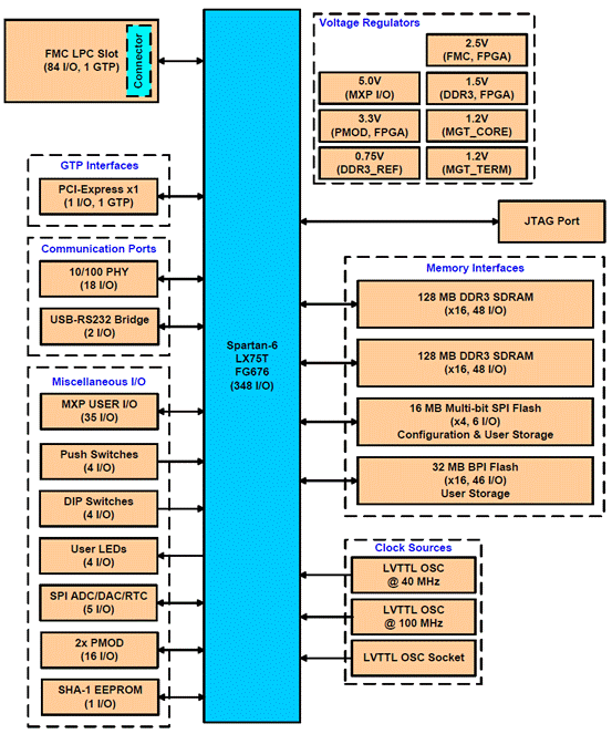
图2.Spartan-6 FPGA LX75T FPGA开发板方框图
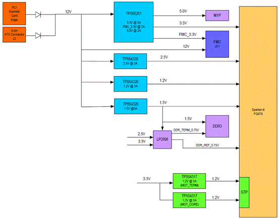
图3.Spartan-6 FPGA LX75T FPGA开发板电源框图
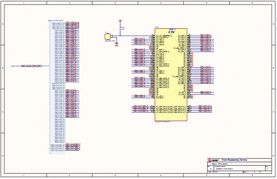
图4.Spartan-6 FPGA LX75T FPGA开发板电路图(1)
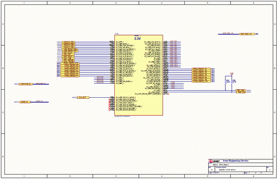
图5.Spartan-6 FPGA LX75T FPGA开发板电路图(2)

图6.Spartan-6 FPGA LX75T FPGA开发板电路图(3)

图7.Spartan-6 FPGA LX75T FPGA开发板电路图(4)
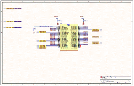
图8.Spartan-6 FPGA LX75T FPGA开发板电路图(5)
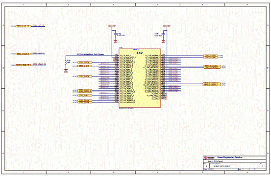
图9.Spartan-6 FPGA LX75T FPGA开发板电路图(6)
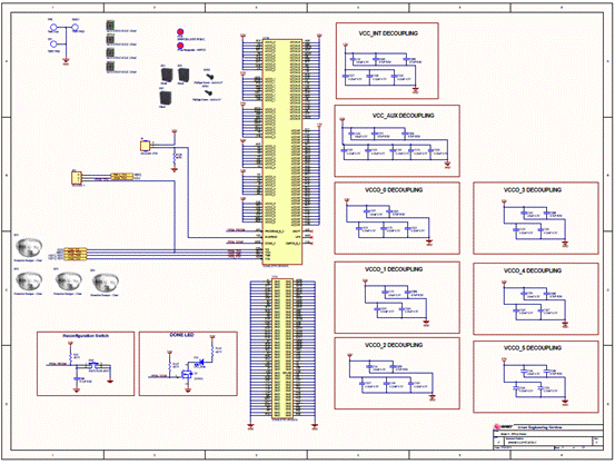
图10.Spartan-6 FPGA LX75T FPGA开发板电路图(7)
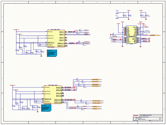
图11.Spartan-6 FPGA LX75T FPGA开发板电路图(8)
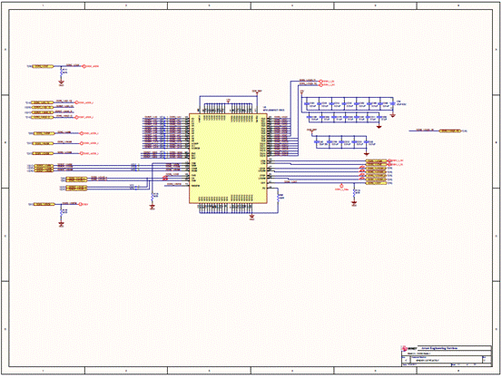
图12.Spartan-6 FPGA LX75T FPGA开发板电路图(9)

图13.Spartan-6 FPGA LX75T FPGA开发板电路图(10)
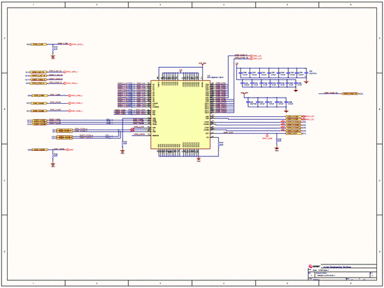
图14.Spartan-6 FPGA LX75T FPGA开发板电路图(11)
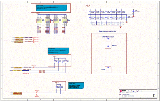
图15.Spartan-6 FPGA LX75T FPGA开发板电路图(12)
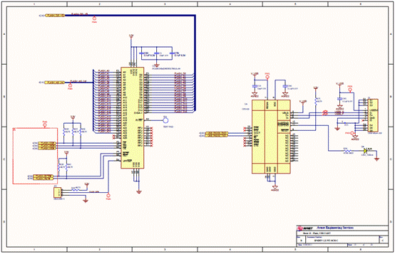
图16.Spartan-6 FPGA LX75T FPGA开发板电路图(13)

图17.Spartan-6 FPGA LX75T FPGA开发板电路图(14)

图18.Spartan-6 FPGA LX75T FPGA开发板电路图(15)
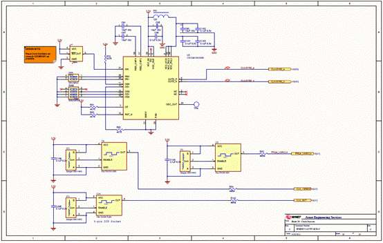
图19.Spartan-6 FPGA LX75T FPGA开发板电路图(16)
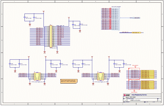
图20.Spartan-6 FPGA LX75T FPGA开发板电路图(17)
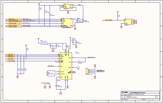
图21.Spartan-6 FPGA LX75T FPGA开发板电路图(18)

图22.Spartan-6 FPGA LX75T FPGA开发板电路图(19)
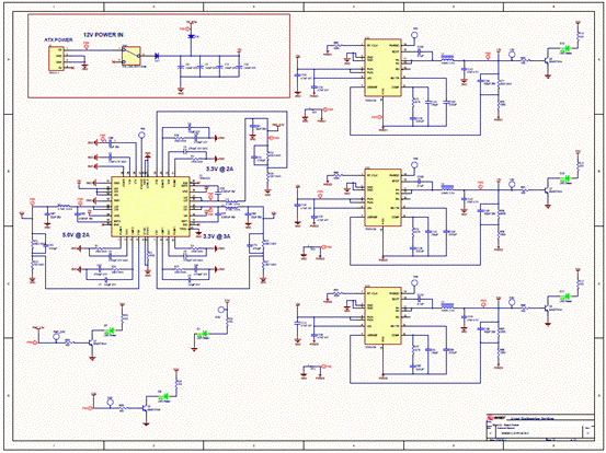
图23.Spartan-6 FPGA LX75T FPGA开发板电路图(20)
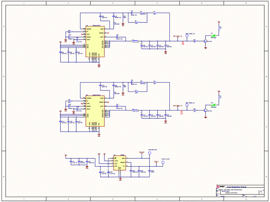
图24.Spartan-6 FPGA LX75T FPGA开发板电路图(21)
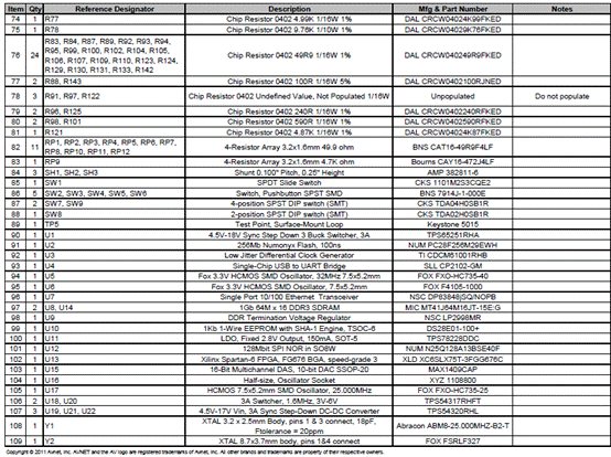
Spartan-6 FPGA LX75T FPGA开发板材料清单:


详情请见:
https://www.em.avnet.com/Support%20And%20Downloads/xlx_s6_lx75t_dev-ug_reva032811.pdf
和
https://www.em.avnet.com/Support%20And%20Downloads/Spartan6_LX75T_Dev_REVC_Schematic.zip
The Spartan-6 LX75T FPGA Development Kit provides a complete hardware environment for designers to accelerate their time to market. The kit delivers a stable platform to develop and test designs targeted to the advanced Xilinx FPGA family. The installed Spartan-6 LX75T device offers a prototyping environment to effectively demonstrate the enhanced benefits of leading edge Xilinx FPGA solutions. Reference designs are included with the kit to exercise standard peripherals on the evaluation board for a quick start to device familiarization.
Spartan-6 FPGA LX75T开发板主要特性:
FPGA
— Xilinx Spartan-6 XC6SLX75T-3FGG676C FPGA
I/O Connectors
— One FMC LPC general-purpose I/O expansion connectors
— One MXP User I/O connector
— Two PMOD connectors
RocketIO™ GTP Transceiver Connectors
— One transceiver supplied on an FMC connectors for use by an expansion module
— One PCI Express add-in card interface (1 lanes @ 2.5 Gbps)
Memory
— 256 MB DDR3 SDRAM components (2 banks of 128 MB x 16)
— 32 MB Parallel Flash (x16)
— 1 Kb EEPROM with SHA-1 Engine
Communication
— USB-RS232 Port
— 10/100 Ethernet port
Power
— Regulated 5.0V, 3.3V, 2.5V, 1.5V and 1.2V supply voltages derived from the PCI Express slot or an external 12 V supply
— SSTL2 Termination Regulators
— Point of Load Regulators for MGT supply rails
Configuration
— 16 MB Multi-bit (x4) SPI Flash
— Xilinx Parallel Cable IV or Platform USB Cable support for JTAG Programming/Configuration
Other
— Four User LEDs
Four User Push Buttons
Four User DIP Switches
— ADC/DAC/RTC combination device
图1.Spartan-6 FPGA LX75T FPGA开发板外形图
图2.Spartan-6 FPGA LX75T FPGA开发板方框图
图3.Spartan-6 FPGA LX75T FPGA开发板电源框图
图4.Spartan-6 FPGA LX75T FPGA开发板电路图(1)
图5.Spartan-6 FPGA LX75T FPGA开发板电路图(2)
图6.Spartan-6 FPGA LX75T FPGA开发板电路图(3)
图7.Spartan-6 FPGA LX75T FPGA开发板电路图(4)
图8.Spartan-6 FPGA LX75T FPGA开发板电路图(5)
图9.Spartan-6 FPGA LX75T FPGA开发板电路图(6)
图10.Spartan-6 FPGA LX75T FPGA开发板电路图(7)
图11.Spartan-6 FPGA LX75T FPGA开发板电路图(8)
图12.Spartan-6 FPGA LX75T FPGA开发板电路图(9)
图13.Spartan-6 FPGA LX75T FPGA开发板电路图(10)
图14.Spartan-6 FPGA LX75T FPGA开发板电路图(11)
图15.Spartan-6 FPGA LX75T FPGA开发板电路图(12)
图16.Spartan-6 FPGA LX75T FPGA开发板电路图(13)
图17.Spartan-6 FPGA LX75T FPGA开发板电路图(14)
图18.Spartan-6 FPGA LX75T FPGA开发板电路图(15)
图19.Spartan-6 FPGA LX75T FPGA开发板电路图(16)
图20.Spartan-6 FPGA LX75T FPGA开发板电路图(17)
图21.Spartan-6 FPGA LX75T FPGA开发板电路图(18)
图22.Spartan-6 FPGA LX75T FPGA开发板电路图(19)
图23.Spartan-6 FPGA LX75T FPGA开发板电路图(20)
图24.Spartan-6 FPGA LX75T FPGA开发板电路图(21)
Spartan-6 FPGA LX75T FPGA开发板材料清单:
详情请见:
https://www.em.avnet.com/Support%20And%20Downloads/xlx_s6_lx75t_dev-ug_reva032811.pdf
和
https://www.em.avnet.com/Support%20And%20Downloads/Spartan6_LX75T_Dev_REVC_Schematic.zip
此内容为AET网站原创,未经授权禁止转载。