
文献标识码: A
文章编号: 0258-7998(2013)09-0061-02
随着印制电路板(PCB)集成度的提高,寄生参数会破坏PCB电源分配网络(PDN)的稳定性[1],PDN的阻抗ZPDN会产生尖峰(反谐振点),参考文献[2]通过去耦电容削弱ZPDN的尖峰并将其推移至PCB的非工作频段,指出了并联去耦电容的等效特性阻抗会产生反谐振点,且该点不可以大于目标阻抗。参考文献[3]总结了各种电容器随着频率升高,其特性阻抗、有效容值受寄生电阻的影响;参考文献[4]是从场角度研究电容特性阻抗与寄生参数的关系,参考文献[5]采用运算放大器来增加电容的有效容值。以上文献都均未给出寄生参数和去耦电容特性阻抗反谐振点关系的完整模型。
参考文献[6]详细描述了单个电容寄生参数与特性阻抗之间的关系;参考文献[7-8]从等效电路角度计算出了ZPDN尖峰的频率位置;参考文献[9]将PDN等效为微波网络计算出了ZPDN尖峰的频率位置;上述文献中,仅给出了寄生参数变化对反谐振点的影响的仿真图形,并没有给出相应数学模型。
本文主要在参考文献[6,8]的基础上,推导并验证了并联电容特性阻抗反谐振点与电容寄生参数的数学模型,即合理选取最佳去耦电容来尽可能压低反谐振点的阻抗,然后在Cadence开发环境中实施了该方法,从而在选取去耦电容器这一环节上给出了重要的理论参考。
1 电容特性阻抗分析
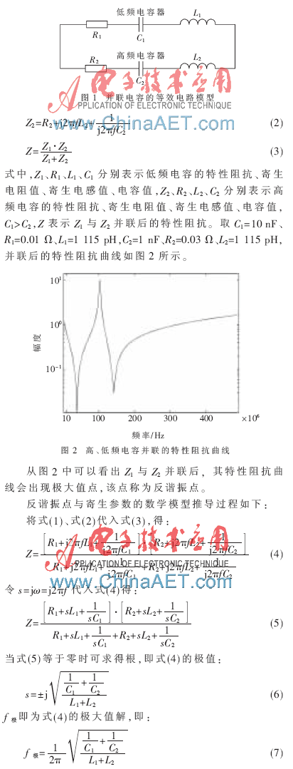
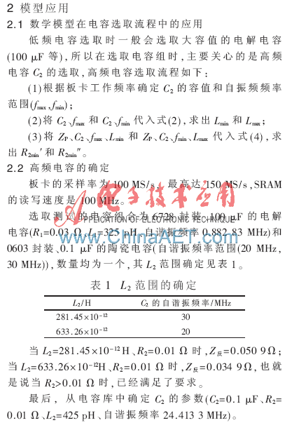
图1为并联电容的等效电路模型[7],阻抗为:
本文从并联电容的等效电路模型出发,推导出电容参数与反谐振点频率、反谐振点幅度的数学模型,然后将此模型应用到基于目标阻抗的设计中。通过简单计算,验证了电容组选取的合理性。此方法简单直观,为高速电路设计人员在选择去耦电容时提供了有价值的参考。
参考文献
[1] POPOVICH M,FRIEDMAN E G,SOTMAN M,et al.On chip power distribution grids with multiple supply voltages for high-performance integrated circuits[J].IEEE Transactions on Very Large Scale Integration(VLSI) Systems,2008,7(16):908-921.
[2] SMITH L D,ANDERSON R E,FOREHAND D W,et al. Power distribution system design methodology and capacitor selection for modern CMOS technology[J].IEEE Transactions on Adcanced Packaging,1999,3(22):284-291.
[3] CHARANIA T,OPAL A,SACHDEV M.Analysis and design of on-chip decoupling capacitors[J].IEEE Transactions on Very Large Scale Integration(VLSI) Systems,2012:1-11.
[4] JIAO D,KIM J H,He Jianqi.Efficient full-wave characterization of discrete high-density multiterminal decoupling capacitors for high-speed digital systems[J].IEEE Transactions on Adcanced Packaging,2008,31(1):154-162.
[5] Gu Jie,HARJANI R,KIM C H.Design and implementation of active decoupling capacitor circuits for power supply regulation in digital ICS[J].IEEE Transactions on Very Large Scale Integration(VLSI) Systems,2009,17(2):292-301.
[6] NOVAK I,NOUJEIM L M,CYR V S,et al.Distributed matched bypassing for board-level power distribution
networks[J].IEEE Transactions on Adcanced Packaging,2002,2(25):230-243.
[7] POPOVICH M,FRIEDMAN E G.Decoupling capacitors for multi-voltage power distribution systems[J].IEEE Transactions on Very Large Scale Integration(VLSI) Systems,2006,14(3):217-228.
[8] KIM J,SHRIGARPURE K,Fan Jun,et al.Equivalent circuit model for power bus design in multi-layer PCBs with via arrays[J].IEEE Microwave and Wireless Components Letters,2011,21(2):62-64.
[9] Zhang Yaojiang,OO Z Z,Wei Xingchang,et al.Systematic microwave network analysis for multilayer printed circuit boards with vias and decoupling capacitors[J].IEEE Transactions on Electromagnetic Compatibility,2010,52(2):401-409.