
标称-48V的电源广泛地用于无线基站和其他网络中心站的通讯设备,能在-48V到-60V范围内变化。测量其电流典型地需要±15V双电源供电的器件。不使用负电源可以减少系统的复杂程度和费用。本设计方案使用Analog Devices公司的AD629差分放大器和AD8603运算放大器,测量-48V到-60V的电流,且仅需要单一正电源供电(参考文献1和2)。
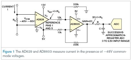
图1显示了AD629和AD8603如何在-48V共模电压面前测量电流。下面的公式表明AD629差分放大器能调节超过电源范围的电压:VCOM_MAX=20×(VS–1.2)–19×VREF, 和VCOM_MIN=20×(–VS+1.2)–19×VREF。共模输入范围为–71到+121V,带一个5V参考电压。电流I流过分流电阻Rs,由差动放大器形成微分电压。AD629固定为1倍增益,那么输出电压为I×RS+VREF。AD8603执行减法器的功能,所以可以抵消共模电压VREF,将增益应用到有用信号I×RS。以20因数放大信号到ADC的2.5V全量程范围。
本设计方案使用AD8603,因为其具有低输入偏置电流和低偏移量漂移。此外,轨对轨输出允许其和ADC分享同一个电源。这个阶段,减法器抵消了电压参考的5V共模信号。形成减法器的四个电阻必须具有与获得最大共模抑制比相匹配的比例。如果不能得到适合的匹配电阻,可以使用AD623单电源仪表放大器替代AD8603,确保高共模抑制比。
两个放大器的偏移量、输入偏置电流和共模抑制比误差,导致AD8603输出的最大误差为163mV。这个计算假设电阻为0.01%的匹配率。该电路经历过并联50、100和200mΩ的Rs来检证。
英文原文:
Single-supply circuit measures –48V high-side current
This circuit measures ?48V high-side current using a single positive supply.
Wenshuai Liao, Analog Devices, Beijing, China; Stephen Lee, Analog Devices, Wilmington, MA; and Yanhui Zhao, Beihang University, Beijing, China; Edited by Charles H Small and Fran Granville -- EDN, 2/21/2008
The nominal –48V rail, which finds wide use in wireless base stations and other telecommunications equipment in network central offices, can vary from –48 to –60V. Measuring its current draw typically requires components that operate on ±15V dual supplies. Eliminating the negative supply would reduce system complexity and cost. This Design Idea uses an AD629 difference amplifier and an AD8603 operational amplifier, both from Analog Devices, to measure current at –48 to –60V and operates from a single positive-power supply (reference 1 and reference 2).
Figure 1 shows how the AD629 and AD8603 measure current in the presence of a –48V common-mode voltage. The following equations demonstrate how the AD629 difference amplifier can condition voltages beyond its supply ranges: VCOM_MAX=20×(VS–1.2)–19×VREF, and VCOM_MIN=20×(–VS+1.2)–19×VREF. With a 5V reference, the common-mode input range is –71 to +121V. The current, I, flows through the shunt resistor, RS, causing a differential voltage, which the difference amplifier senses. The AD629 has a fixed gain of one, so the output voltage is I×RS+VREF. The AD8603 functions as a subtractor so that it can reject the common-mode voltage, VREF, and apply gain to the signal of interest, I×RS. A factor of 20 amplifies the signal to span the 2.5V full-scale range of the ADC.
This Design Idea uses the AD8603 because it has low input-bias current and low offset drift. In addition, the rail-to-rail output allows it to share the same supply as the ADC. In this stage, the subtractor rejects the 5V common-mode signal from the voltage reference. The four resistors that form the subtractor must have matched ratios to obtain maximum common-mode rejection. If you cannot obtain tightly matched resistors, you can use an AD623 single-supply instrumentation amplifier in place of the AD8603, ensuring high common-mode rejection.
Offset, input-bias-current, and common-mode-rejection errors from both amplifiers result in a 163-mV maximum error at the output of the AD8603. This calculation assumes resistors with a 0.01% ratio match. The circuit was verified on the bench using 50-, 100-, and 200-mΩ shunts for RS.
References
“High Common-Mode Voltage, Difference Amplifier AD629,” Analog Devices, 1999 to 2007.
“Precision Micropower, Low Noise CMOS Rail-to-Rail Input/Output Operational Amplifiers AD8603/AD8607/AD8609,” Analog Devices, 2005.