
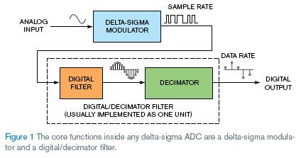
Σ-Δ转换器在从直流到几MHz信号的宽频率范围内,都能理想的实现高分辨率信号转换。图1显示了Σ-ΔADC的基本拓扑或核心,其内部为Σ-Δ调节器和数字滤波器的串联。研究Σ-ΔADC时,可以发现虽然它们具有多种特色,但都为这种基本架构。这个窗和后面的三个Baker最佳窗研究了基本拓扑和这两个模块的功能。
Σ-ΔADC的输入信号为交流或直流电压。这个和后三个Baker最佳窗使用单周期正弦波作为输入信号。使用1位内部ADC,图1中内部转换调节器采集输入信号,产生粗量化的输出作为输入信号。调节器将模拟输入信号转换为高速脉冲波形。调节器输出脉冲序列一到零的比例反映了输入模拟电压。虽然调节器产生一个带噪声的输出,但是未来的列说明电路将噪声“塑造”成更高频率的输出频谱。这个动作为数字滤波器输出的低噪声、高分辨率转换铺平了道路。
在调节器输出,数字滤波器解决了高频噪声和高速采样率的问题。因为信号位于数字域,可以采用低通数字滤波器削弱高频率噪声,采用抽取滤波器减小输出数据的速度。数字/抽取滤波器采样和滤除调节器1位代码
串,并创建低速多位编码。
虽然大多数转换器只有一个采样率,Σ-Δ转换器却有两个:输入采样率和输出数据率。这两个有意义的变量比例定义了系统抽取比例。抽取率和转换器有效分辨率之间存在一个强大的关系。未来的窗将检测调节器、数字/抽取滤波器和可调节抽取比例怎样工作。
英文原文:
Delta-sigma ADCs in a nutshell
Part one of a three-part series exploring the basic topology and functions of delta-sigma ADCs.
By Bonnie Baker -- EDN, 12/14/2007
MORE AT EDN.COM
Click here to read many more of this author's columns.
Delta-sigma converters are ideal for converting signals over a wide range of frequencies from dc to several megahertz with very-high-resolution results. Figure 1 shows the basic topology, or core, of a delta-sigma ADC, which has an internal delta-sigma modulator in series with a digital filter. As you explore delta-sigma ADCs, you will find that, although they have a variety of other features, they all possess this basic structure. This column and the next three Baker’s Best columns explore the basic topology and functions of these two modules.
The input signal to the delta-sigma ADC is an ac or dc voltage. This and the next three Baker’s Best columns use a single cycle of a sine wave as the input signal. Using a 1-bit internal ADC, the internal converter modulator in Figure 1 samples the input signal, producing a coarse, quantized output. The modulator converts the analog-input signal into a high-speed, pulse-wave representation. The ratio of ones to zeros in the modulator’s output pulse train mirrors the input-analog voltage. Although the modulator produces a noisy output, future columns will show that the circuit “shapes” this noise into the higher frequencies of the output spectrum. This action paves the way for a low-noise, high-resolution conversion at the output of the digital filter.
At the modulator output, the digital filter addresses high-frequency noise and high-speed-sample-rate issues. Because the signal now resides in the digital domain, you can apply a lowpass digital filter to attenuate the higher frequency noise and a decimator filter to slow down the out
put-data rate. The digital/decimator filter samples and filters the modulator’s stream of 1-bit codes and creates a slower multibit code.
Although most converters have only one sample rate, delta-sigma converters have two: the input sampling rate and the output-data rate. The ratio of these two meaningful variables defines the system’s decimation ratio. A strong relationship exists between the decimation ratio and the converter’s effective resolution. A future column will examine how the modulator, digital/decimator filter, and adjustable decimation ratio work.
Reference
Baker, R Jacob, CMOS Mixed-Signal Circuit Design: Volume II, John Wiley & Sons, 2002, ISBN: 0471227544.