
《电子技术应用》
您所在的位置:首页 > EDA与制造 > 设计应用 > 基于仿射变换参数优化的多维度电流分布快速重构方法及应用
基于仿射变换参数优化的多维度电流分布快速重构方法及应用
电子技术应用
张瑾1,符义琴2,赵海健1,谢业磊1,张阔1,吴浩1,张建国1,庄哲民3
1.深圳市中兴微电子技术有限公司;2.南京信息工程大学; 3.上海楷登电子科技有限公司
摘要: 针对芯片封装设计早期缺乏联合电流分析模型、仿真迭代周期长的痛点,提出一种基于仿射变换参数优化的多维度直流电流分布快速重构方法。该方法设计一套多模板兼容的可扩展损失函数,在芯片级,通过拟合已知功能模块的电流分布,优化仿射变换参数以重构出全芯片的电流分布云图;在封装级,通过同步优化多芯片相对于封装的仿射变换参数,以最小化布局匹配误差,从而将多个独立的芯片电流分布云图精准合成为系统级联合电流分布云图。然后,设计实现相关GUI工具,建立从“模块→芯片→封装”全链路映射框架,无需详细版图,即可在15 min内生成覆盖芯片到封装的多维度电流分布,较传统后仿建模流程提速30倍。实验表明,该方法能在芯片设计早期精准捕捉压降热点与电迁移风险区域,为芯片封装电源设计提供高置信度的早期探索与快速验证手段。
中图分类号:TN402 文献标志码:A DOI: 10.16157/j.issn.0258-7998.260804
中文引用格式: 张瑾,符义琴,赵海健,等. 基于仿射变换参数优化的多维度电流分布快速重构方法及应用[J]. 电子技术应用,2026,52(8):52-56.
英文引用格式: Zhang Jin,Fu Yiqin,Zhao Haijian,et al. Rapid reconstruction method for multi‑dimensional current distribution based on affine‑transformation parameter optimization and application[J]. Application of Electronic Technique,2026,52(8):52-56.
Rapid reconstruction method for multi‑dimensional current distribution based on affine‑transformation parameter optimization and application
1.Department of Packaging and Testing, Sanechips Technology Co.,Ltd.;2.Nanjing University of Information Science and Technology; 3.Shanghai Cadence Electronics Technology Co., Ltd.
Abstract: In the early stage of chip-package co-design, there is no joint current analysis model and the pain point of long simulation iteration period. This paper proposes a fast reconstruction method of multi-dimensional DC current distribution based on affine transformation parameter optimization. This method designs a set of extensible loss functions compatible with multiple templates. At the chip level, by fitting the current distribution of known functional modules, the affine transformation parameters are optimized to reconstruct the current map of the entire chip. At the package level, the affine transformation parameters of multiple chips relative to the encapsulation are optimized synchronously to minimize the layout matching error and accurately integrate the current maps of multiple independent chips into the system-level joint current distribution. Then, relevant GUI tools are designed and implemented to establish a full-link mapping framework from "module → chip → encapsulation". The multi-dimensional current distribution from the coverage chip to the encapsulation can be generated within 10 minutes without the need of detailed layout, which is 30 times faster than the traditional post-simulation modeling process. Experiments show that this method can accurately capture voltage drop hotspots and electromigration risk areas in the early stage of chip design, and provide early exploration and rapid verification methods with high confidence for chip encapsulation power supply design.
Key words : affine transformation;current distribution reconstruction;voltage drop and electromigration

引言

随着人工智能、高性能计算及5G通信等领域的迅速发展,多芯片封装的需求日益增长,半导体工艺逐步进入纳米尺度。这使得芯片系统复杂度不断提升,系统级电流分布愈发复杂,压降与电迁移问题成为制约性能与可靠性的关键,芯片与封装的电源完整性设计面临巨大的挑战[1]。传统的电源完整性分析依赖于设计后期详细的版图提取和全波电磁仿真,其过程计算密集,导致整体耗时较长。在设计后期一旦发现压降超标或电迁移风险,亟需进行昂贵的版图返工。因此,在芯片与封装的架构设计及早期布局阶段,如果能找到一种电流分布快速重构的方法及时定位设计风险,这对提升电源完整性设计的效率、减少返工和节约成本有关键作用,具有较高的工程与商业价值。

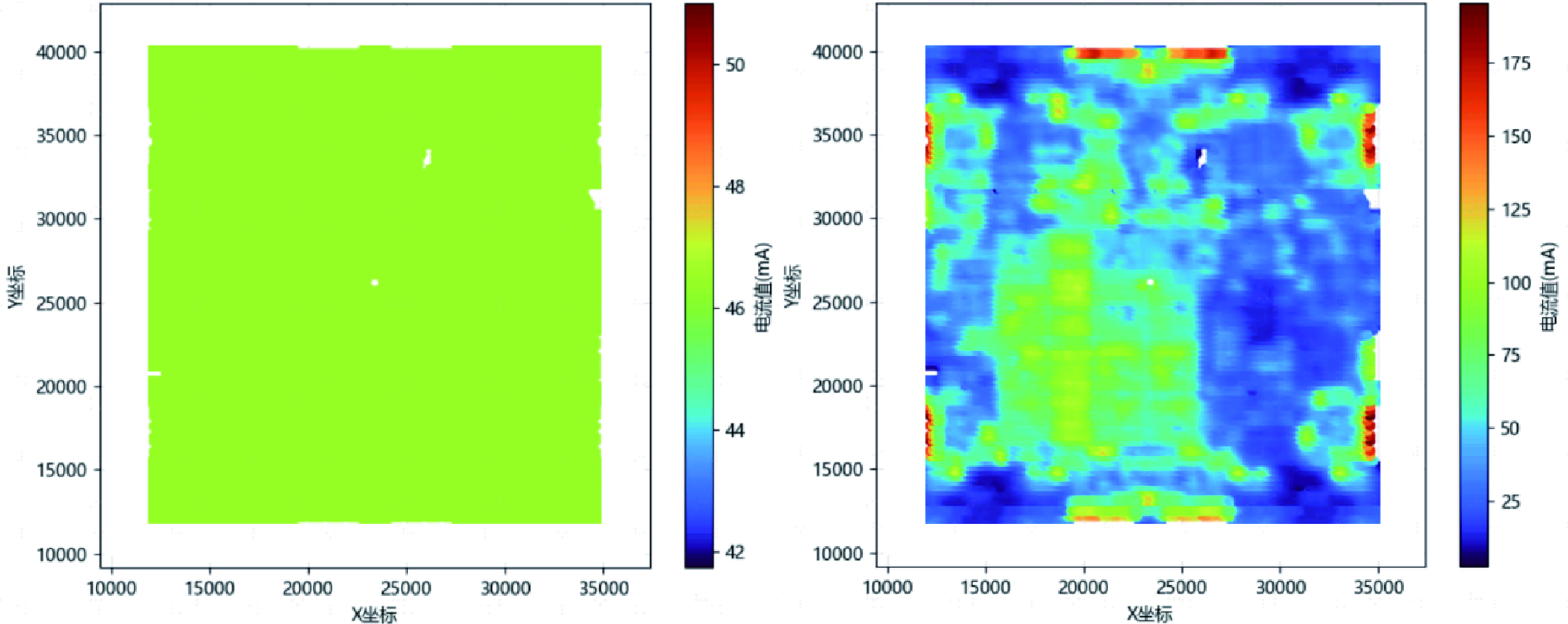
当前主流的电流分布模型主要包括均流模型和电流分布模型。如图1所示,均流模型是一种简化模型,将总电流均分到所有电源管脚,每个管脚的电流值相同,计算速度快,但仿真精度较低,无法反映实际电路中功能模块之间电流分布不均的特性,常用于简单负载场景;电流分布模型为每个电源管脚分配不同的电流值,能够反映功能模块之间的实际电流分布,是目前最常用的模型[2]。但是,电流分布模型中不同电流值的分配依赖后期生成的电流分布文件,且整个模型的提取占用大量的计算资源和时间。
图片1.png

图1 均流模型和电流分布模型

仿射变换能够描述空间坐标的平移、旋转和缩放,广泛应用于计算机视觉、图形学及地理信息系统等领域,并取得不错的研究成果[3]。芯片内部功能模块之间多次复用,相同功能模块之间存在平移、旋转或镜像关系。多芯片合封场景,相同功能芯片之间也存在平移或旋转关系。基于此,本文提出一种基于仿射变换参数优化的多维度电流分布快速重构方法,实现芯片级电流分布云图重构与封装级多芯片电流分布云图合成,配套开发的GUI工具可在15 min内完成分析和处理,较传统方法提速30倍。实验验证表明,该方法能有效识别早期压降热点与电迁移风险,为电源完整性设计提供高效验证手段。


本文详细内容请下载:

https://www.chinaaet.com/resource/share/2000007209


作者信息:

张瑾1,符义琴2,赵海健1,谢业磊1,

张阔1,吴浩1,张建国1,庄哲民3

(1.深圳市中兴微电子技术有限公司,广东 深圳 518055;

2.南京信息工程大学,江苏 南京 210044;

3.上海楷登电子科技有限公司,上海 200000)

2.jpg

此内容为AET网站原创,未经授权禁止转载。