
简单的RC低通滤波器允许微处理器单输出端口扩展输出位数
摩尔定律形成一个几乎必然的推论——下一年,微处理器将会拥有更多的功能,而软件团队则会提出更多创意。然而不幸的是,微处理器输出端口仍保持原样。找到一个用作测试、调试或是标准I/O口的空闲输出端是件相当困难的事。外加简单硬件,如图1所示电路实现单端口“总线”,提供无限量的并行输出端。
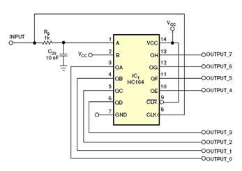
图1 HC164外围电路图
带RC低通滤波器的微处理器输出端控制串并转换器HC164。为了数据输入到串并转换器,每位都要由1-0-1的转换组成,这种转换数据低电平状态长度是变化的。如果低电平状态超出了低通滤波器的时间常数,一个零移进寄存器;如果低电平状态短,一个1就移进寄存器。这样,时钟信号和数据信号就合并成为一个信号。低通滤波器可以分离时钟信号和数据信号(如图2)。
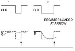
图2 时钟信号与数据信号合并成一个信号
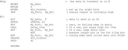
表1 whip程序输出功能
如表1所示,一个简单的“whip”程序实现8位输出功能。假定低通滤波器时间常数为3μs,使用4MHz或更高频率晶振时,指令时间应该为1μs或更短。程序使用My_Port端口的My_ Bit输出的位操作。
如图1中电路可以控制一些低速设备,例如继电器或LCD,但是电路用于发光二极管时,HC164进行写操作会产生令人讨厌的闪烁。为解决这个问题,图3电路使用另一款串入并出寄存器4096,这种芯片有滤波输入功能,允许全部没有达到临时水准的输出同时更新。两个单稳态电路提供数据和滤波信号。这个电路可以用来控制并行设备,例如基于HD44780的显示模块。
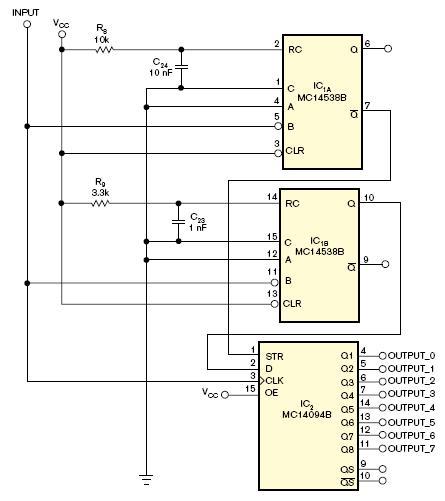
图3 串行输入/并行输出芯片4096外围电路图
附英文原文:
RC lowpass filter expands microcomputer’s output port
A simple lowpass RC filter allows a single output pin of a microcontroller to expand the number of output bits.
Rex Niven, Forty Trout Electronics, Eltham, Victoria, Australia; Edited by Charles H Small and Fran Granville -- EDN, 6/21/2007
It’s almost a corollary to Moore’s Law: Next year, microcomputers will have more features, and the software team will have bigger ideas. Unfortunately, though, the number of output pins will stay the same. Finding even one spare output for diagnostics, test, or even standard I/O can be a tussle. The single-pin “bus” in Figure 1 can provide an unlimited number of parallel outputs with simple additional hardware. A microcomputer output with an RC lowpass filter controls serial-to-parallel converter HC164. To enter data into the serial-to-parallel converter, each bit consists of a one-to-zero-to-one transition, which alters the length of the low state. If the low state is longer than the lowpass filter’s time constant, a zero shifts into the register. If the low state is short, then a one shifts into the register. The clock and data signals thus combine into one signal. A lowpass filter separates the clock and data signals (Figure 2).
Listing 1, a simple “Whip” routine, performs the output function for eight bits. Assume that the RC time constant is 3 µsec, and the instruction time should be 1 µsec or less at a crystal frequency of 4 MHz or greater. The routine uses bitwise manipulation of output My_Bit of port My_Port.
Although the circuit in Figure 1 can control slow-reacting devices, such as relays or LCDs, using it with LEDs can give an annoying flicker when the HC164 is writing. To address tha
t problem, the circuit in Figure 3 uses another serial-in/parallel-out register, the 4094, which has a strobe input to allow simultaneous updates of all outputs without temporary levels. A twin monostable circuit supplies the data and strobe signals. This circuit should be able to control parallel devices, such as display modules based on HD44780 devices.